Το δημοσίευσε το VLSI Symposia tipsheet με περισσότερες λεπτομέριες για τον Sony κυρτό αισθητήρα με σχεδιάγραμμα..

Για να δούμε και τεχνικά τι έχει να φέρει η τεχνολογία στις φωτογραφικές μας μηχανές…
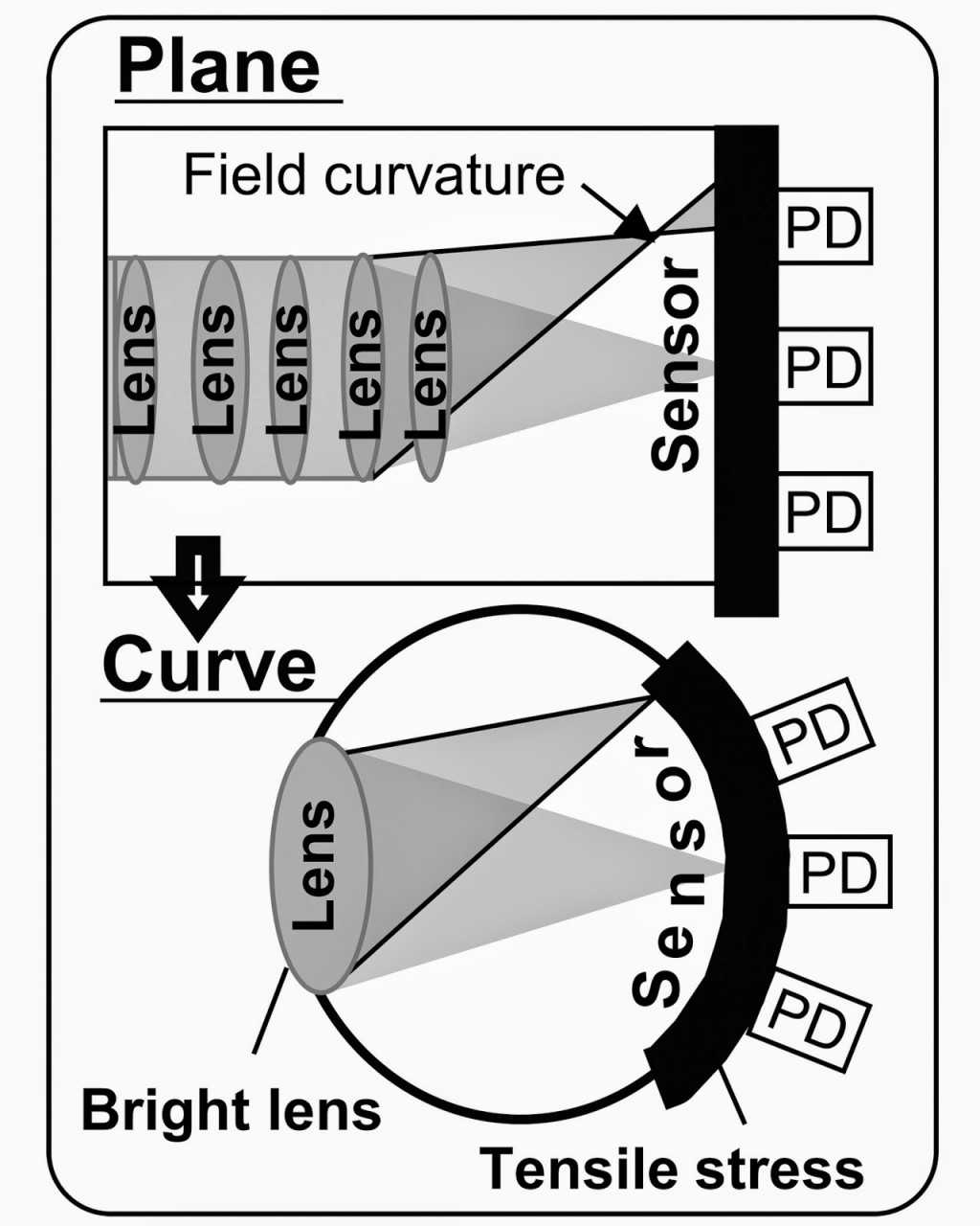
“Curved CMOS Image System: When light transmitted by a lens strikes a perpendicular target such as a CMOS image sensor, it forms a circle of light called an image circle. It’s difficult for a flat (planar) CMOS image sensor to deliver high image sensitivity at high resolution (highly scaled pixel pitch) because of the fundamental physical limit known as quantum efficiency. To break through that physical limit and to achieve higher sensitivity anywhere within the image circle at higher resolution, Sony built and will describe an imaging system that comprises a hemispherically curved, back-illuminated CMOS image sensor (BIS) and integrated lens. It doubles the sensitivity at the edge of the image circle while increasing sensitivity at its center by a factor of 1.4, with a 5x reduction of dark current (Jd) compared to a planar BIS. Moreover, a common problem known as lens field curvature aberration (Afc) is mitigated by the curved sensor itself, and so the curved BIS enables higher system sensitivity with a brighter lens with a smaller F number (Fn) than is possible with a planar BIS. In addition, by controlling the tensile stress of the BIS chip to produce a curved shape in the first place, the energy band-gap (Eg) is widened and a lower Jd is achieved. (Paper T2.1, “A Novel Curved CMOS Image Sensor Integrated with Imaging System,” K. Itonaga et al., Sony)”